Graphene is a carbon allotrope which is touted as the wonder material with applications ranging from high capacity batteries to transparent electronics to bio-compatible medical components. You can read more about the potential applications over on Wikipedia. There are too many to list here.
Researchers at the University of Nottingham, UK, have found a way to print the wonder-material via ink jet technology, which may lead to electronic applications such as photovoltaic devices.
Graphene
Graphene is not fantastically difficult to manufacture in single layers. The guys who invented it (and won the Nobel Prize for their work) first manufactured it by placing sticky tape onto graphite (as found in pencil lead) and ripping the tape off to create thin flakes of graphene.
They continued experimentation, and gradually managed to reduce the thickness of these graphite flakes until eventually they produced flakes just 1 atom thick, making graphene the thinnest and strongest material on Earth.
But forming those layers into 3D shapes, or stacking them like CFRP layers into a sandwich structure has proven to be tricky (and by tricky, we mean “labour intensive”.
With the aid of quantum mechanical modelling they were able to determine exactly how electrons flow between the layers. Now with 3D printing they are able to guide the structure so that the behavior of those electrons is controlled the way they want it. Precision!
By linking together fundamental concepts in quantum physics with state-of-the art-engineering, we have shown how complex devices for controlling electricity and light can be made by printing layers of material that are just a few atoms thick but centimetres across Professor Mark Fromhold, Head of the School of Physics and Astronomy
“According to the laws of quantum mechanics, in which the electrons act as waves rather than particles, we found electrons in 2D materials travel along complex trajectories between multiple flakes. It appears as if the electrons hop from one flake to another like a frog hopping between overlapping lily pads on the surface of a pond”, said Professor Fromhold.
While 2D layers and devices have been 3D printed before, this is the first time anyone has identified how electrons move through them and demonstrated potential uses for the combined, printed layers.
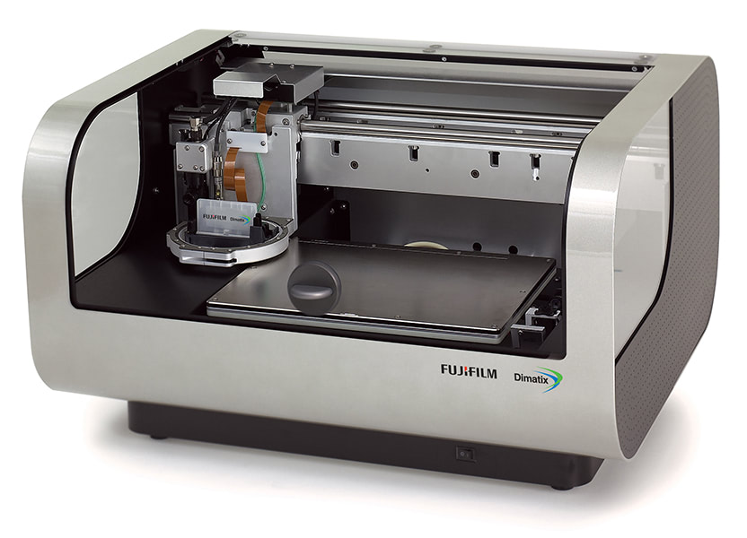
So far the team has managed to use the Inkjet-printed graphene to make a field effect transistor and contacts on a phototransistor. They did so with a Fujifilm Dimatix DMP‐2800 inkjet printer, which has been designed for printing materials and is used a lot in MEMS manufacturing.
“Our results could lead to diverse applications for inkjet-printed graphene-polymer composites and a range of other 2D materials. The findings could be employed to make a new generation of functional optoelectronic devices; for example, large and efficient solar cells; wearable, flexible electronics that are powered by sunlight or the motion of the wearer; perhaps even printed computers.”
The name of the research paper published is ‘Inter-Flake Quantum Transport of Electrons and Holes in Inkjet-Printed Graphene Devices’ and can be read over at this link for anyone who isn’t baffled by anything with the word “quantum” in it (not me).