Researchers at Purdue University’s College of Engineering have made a significant breakthrough in 3D additive nanoprinting. Led by Liang Pan, a professor of mechanical engineering, the team has developed a patent-pending, single-photon 3D nanoprinting technology that allows for the creation of high-resolution nanostructures faster and at a much lower cost than traditional methods. This innovation is set to transform industries reliant on nanotechnology by enabling more efficient and affordable production of complex structures.

A Leap Forward in Nanoprinting
Traditional laser-based 3D nanoprinting, such as femtosecond laser two-photon polymerization, has long been used to fabricate intricate nanostructures. However, this technique has several drawbacks—it is expensive, slow, and requires high-power lasers, limiting its commercial viability in manufacturing. Purdue’s new technology overcomes these obstacles by eliminating the need for costly femtosecond lasers and single-point scanning processes.
“The technology uses less expensive light sources, such as a simple laser pointer, reducing tool costs by 10 to 100 times,” Pan explained. “The writing speed is exponentially faster for each beam, and we can further expand to parallel scanning with tens or even hundreds of beams.”
This single-photon approach significantly boosts throughput without compromising the resolution, making it a game-changer for various industries, from nanotechnology research and manufacturing to healthcare.
Advantages of Single-Photon 3D Nanoprinting
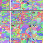
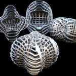
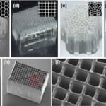
The technology developed by Pan’s team offers several advantages over traditional methods. It not only increases the production speed but also maintains high-resolution output, achieving structures as small as 120 nanometers using a low-cost diode laser. Additionally, the researchers demonstrated parallel nanoprinting by using an array of laser beams, paving the way for even larger-scale production.
By eliminating the need for high-power lasers and complex, time-consuming processes, Purdue’s single-photon method is positioned to make 3D nanoprinting more accessible and cost-effective for both industrial and research applications.
Applications and Future Development
Purdue’s 3D nanoprinting technology has a wide range of potential applications, including nanolithography, zero-stiffness microstructures, and thermal interface structures. These applications are crucial in sectors like electronics, advanced manufacturing, and medical devices.
Looking ahead, Pan’s team is focused on further refining the technology to increase scanning throughput and lower tool costs even further. They have already received two grants from the National Science Foundation to support their ongoing research and development efforts.
The Purdue Innovates Office of Technology Commercialization is actively seeking industry partners to help develop and commercialize the technology. For those interested, they can reach out to Parag Vasekar, business development and licensing manager, for more information on how to get involved.
Purdue’s Commitment to Innovation
This innovative work is part of Purdue University’s broader mission to lead in technological advancement. The Purdue Innovates Office of Technology Commercialization plays a vital role in bringing these forward-thinking developments to market, contributing to the university securing 290 U.S. and international patents in fiscal year 2024.
With this latest advancement in 3D nanoprinting, Purdue continues to expand the possibilities in additive manufacturing, providing solutions that have the potential to reshape industries dependent on nanotechnology.