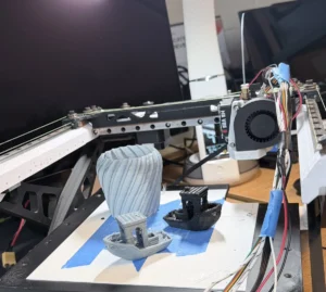
Full-size 3D-printed tungsten tiles survived 74 plasma shots inside San Diego’s DIII-D National Fusion Facility.
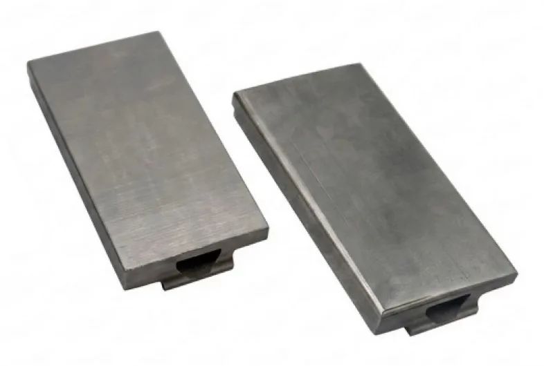
A team from North Carolina State University, Oak Ridge National Laboratory, and JEOL Ltd. printed the divertor tiles by electron-beam powder bed fusion. They finished the parts to DIII-D tolerances and installed them in the machine’s lower divertor in July 2026. Over three days of the Tile Testing Campaign, the surfaces took medium-to-high-power H-mode discharges for about four minutes of total plasma time. The printed tiles came out intact.
Tungsten is a leading choice for plasma-facing hardware because of its high melting point. It is brittle at lower temperatures and hard to form into complex shapes. Laser powder bed builds of tungsten often crack. Several years ago, ORNL and NC State showed that electron-beam powder bed fusion in vacuum can make dense, crack-free tungsten when the bed stays hot above the brittle range.
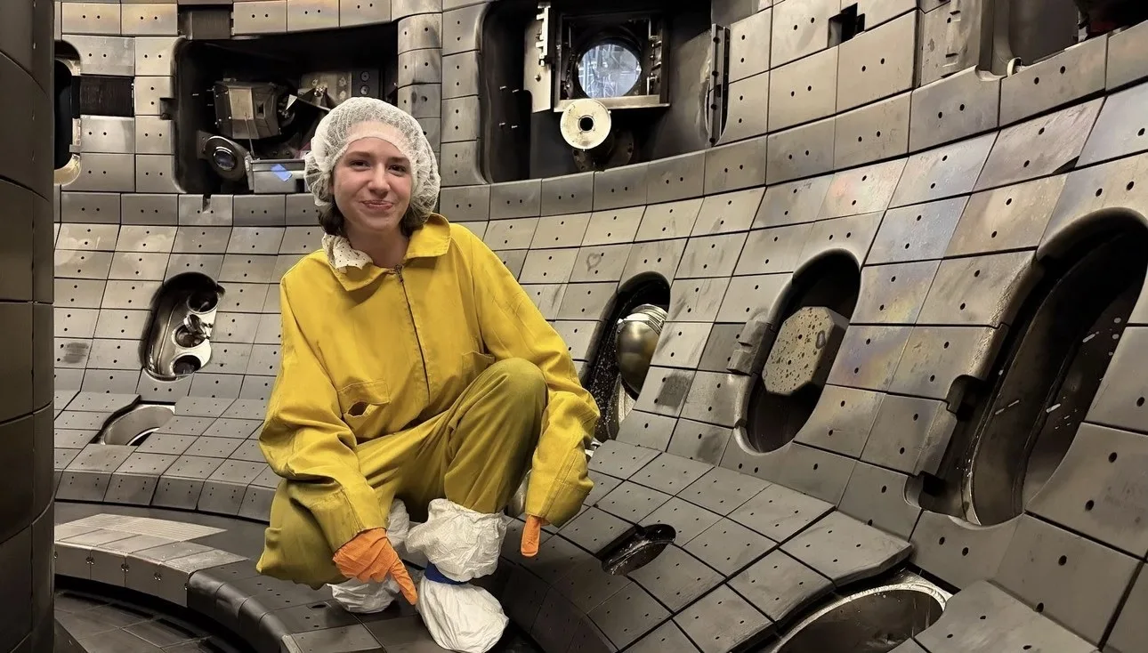
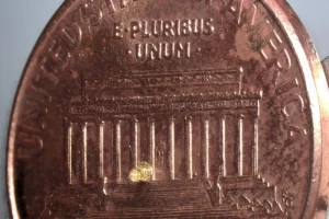
Small printed buttons tested in 2025 on DIII-D’s Divertor Materials Evaluation System saw heat fluxes near 20 MW/m². Brief peaks rose above 35 MW/m², with little surface damage. That result led Sandia National Laboratories’ Jonathan Coburn, who led the novel-tile portion of the 2026 campaign, to ask for a full-size tile.
Scale was the hard part. The DIII-D tile for this work is about 140 by 130 millimeters. NC State’s largest prior tungsten print was about 50 millimeters across. The university’s own machines could not hold the required temperature over a build that large.
“There were major challenges to making this happen. We understood the processing science behind tungsten additive manufacturing and the physics of scaling up. What we needed was the hardware and partners who could move fast. ORNL and JEOL were exactly that,” said Tim Horn, an associate professor at NC State and research director at the Center for Additive Manufacturing and Logistics.
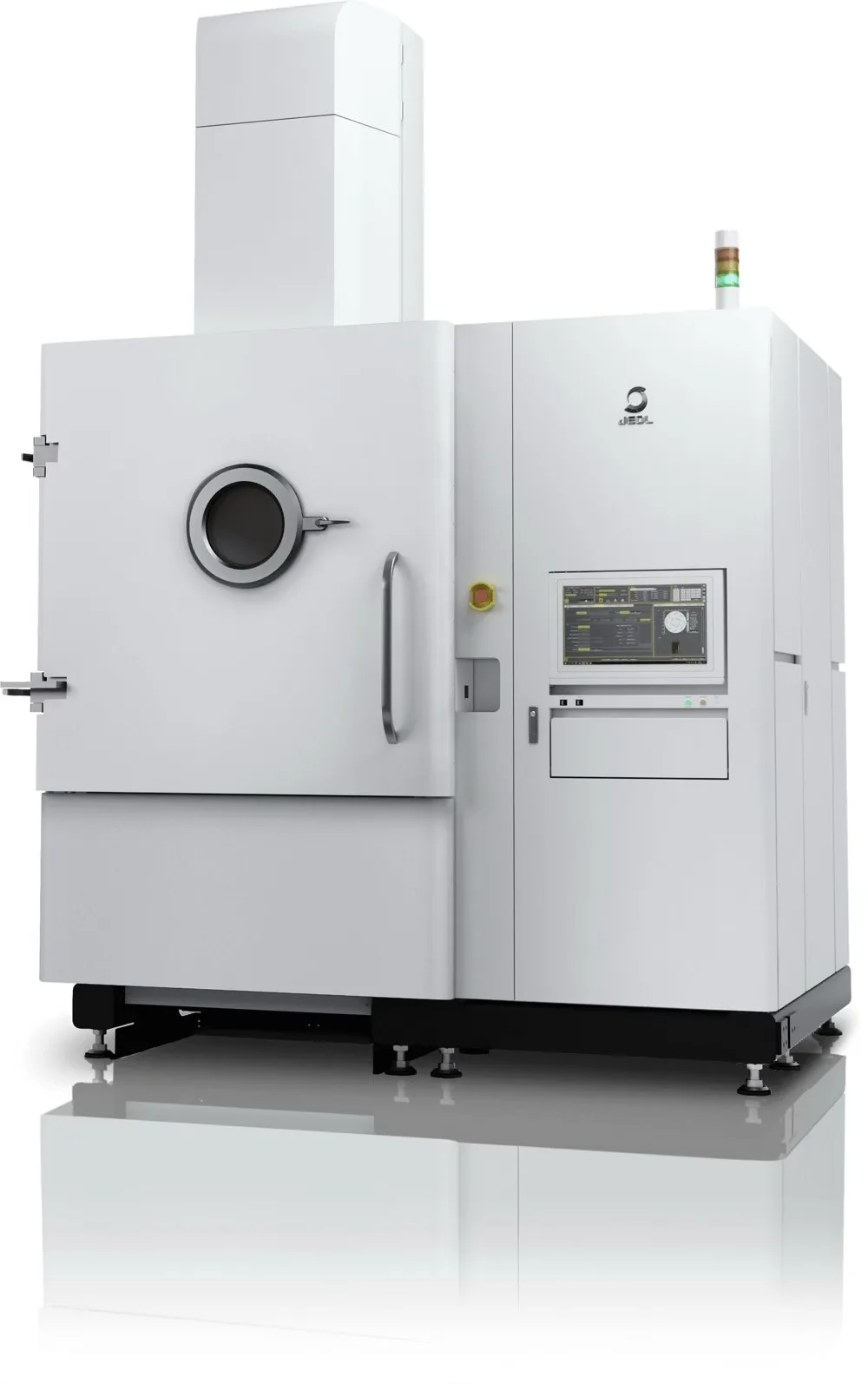
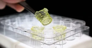
JEOL engineers printed flat and domed designs on a JAM-5200EBM at the company’s facility in Akishima, Japan. ORNL’s Fusion Materials Core Program funded fabrication. After early iterations, the as-printed tiles met design tolerances with no major defects. Back at NC State, postdoctoral researcher Haozhi Zhang and undergraduate Olivia Mehalick finished the parts. Wire electrical discharge machining shaped mounting features. A digital-twin-guided multi-axis grinder then removed about 250 microns from the plasma-facing face.
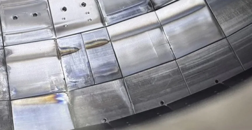
Each finished tile pair is about 136 by 143 millimeters and 20 millimeters thick. Mounted on copper-alloy pedestals, the hardware went from invitation to installed parts in about eight months. A slightly misaligned neighboring conventional tile melted along its leading edge and spattered onto one printed tile, giving an unplanned look at how the printed material responds. Detailed erosion and surface analysis still awaits a radiation survey before the tiles return to NC State.
“Fusion has been called the energy source of the future for a long time. One of the things holding it back is materials that can survive inside the machine,” said Michael Kirka, a researcher at ORNL. “Showing that printed tungsten tiles can go into a working tokamak and come out intact moves additive manufacturing from ‘promising’ to ‘proven’ for fusion.”
Source: JEOL USA